
One Frame for the Big Picture, Zoom in to See the Finest Details
How MindVision’s 410-Megapixel Industrial Camera Redefines Ultra-High-Precision Inspection
One Frame for the Big Picture, Zoom in to See the Finest Details: How MindVision’s 410-Megapixel Industrial Camera Redefines Ultra-High-Precision Inspection
From wafers to panels, from semiconductors to aerospace – when “large field of view” and “high precision” are no longer an either-or choice, a 410-megapixel industrial camera is becoming the game-changer.
 1. The Inspection Dilemma: When “Seeing” Is Not Enough for “Measuring Accurately”
 1. The Inspection Dilemma: When “Seeing” Is Not Enough for “Measuring Accurately”
In the cleanrooms of semiconductor wafer fabs, a high-precision inspection system is scanning a 12-inch wafer. A 5-megapixel camera requires approximately 80 partial captures to cover the entire wafer, with stitching alone consuming over 40% of the total inspection time. Even more critically, missed defects at stitching seams often become a hidden source of yield loss.
On Gen 10.5 display panel production lines, a large-format panel similarly requires dozens of captures and stitching operations. Each mechanical movement introduces new positioning errors, and each stitching operation accumulates uncontrolled system deviations.
In aerial surveying and mapping, conventional area-scan cameras have limited single-frame coverage, resulting in high overlap between flight strips and heavy stitching workloads, making data processing efficiency a bottleneck.
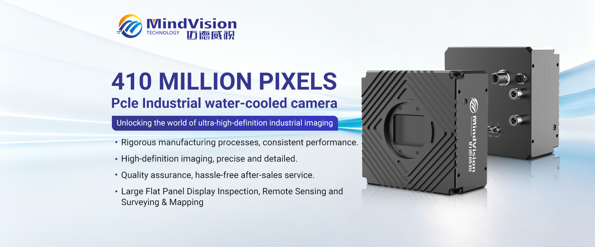
The MindVision MV-PX41000C/M 410-megapixel industrial camera is designed precisely to break this trade-off.
2. Product Overview: 410-Megapixel Industrial Area-Scan Camera
The MV-PX41000C/M is a 410-megapixel industrial area-scan camera featuring the Canon LI8030SA full-frame back-illuminated stacked CMOS image sensor, delivering a resolution of 24,592 × 16,704 – equivalent to 198 times Full HD, 49 times 4K, and 12 times 8K.
The camera is available in colour (MV-PX41000C) and monochrome (MV-PX41000M) versions. It supports the CoaXPress 2.1 protocol standard and is equipped with a TEC thermoelectric cooling plus water-cooling dual-channel precision cooling system, enabling stable, uncompressed, zero-frame-loss output at 8 fps at full resolution.
This product is among the earliest 400-megapixel-class industrial area-scan cameras available worldwide.
3. Core Technical Advantages
3.1 24K Ultra-High Resolution
The sensor integrates 410 million pixels within a 35mm full-frame optical format with a pixel size of 1.5μm × 1.5μm. The monochrome version offers a sensitivity of 12,300 e/lx·s and quantum efficiency of 62.4%; the colour version offers 7,000 e/lx·s and 61.8% quantum efficiency.
The camera supports 14-bit AD conversion, fully preserving grayscale levels in both highlight and shadow regions. Combined with hardware-integrated pixel-wise real-time correction algorithms, it maintains highly uniform image quality from centre to edge.
3.2 CXP-12 Ultra-High-Speed Data Transmission
A single 14-bit frame contains approximately 123 MB of data, and the 8 fps data stream reaches approximately 984 MB/s. The MV-PX41000C/M adopts the CXP-12 interface standard with 4-channel aggregated bandwidth of 48 Gbps, supporting uncompressed, zero-frame-loss output at full resolution and 8 fps.
Interface design highlights:
- HD-BNC industrial standard connectors with coaxial cable transmission distances from 10 to 65 metres
- PoCXP (Power over CoaXPress) support, enabling simultaneous image transmission, external triggering, and power supply over a single coaxial cable
- Effectively simplifies on-site cabling and reduces system integration complexity
3.3 TEC + Water-Cooling Dual-Channel Precision Cooling
High-density sensors generate heat build-up under sustained high-load operation, increasing dark current noise. The MV-PX41000C/M employs TEC thermoelectric cooling plus water-cooling dual-channel active cooling to achieve closed-loop temperature control. Test data indicates that this solution reduces sensor dark current noise by over 90%.
3.4 Industrial-Grade Reliability
- All-metal housing: Provides shock and interference resistance while serving as a passive heat dissipation path
- IP40 protection rating: Suitable for laboratory and cleanroom environments
- Operating temperature range: 0~50°C
- M58×0.75 industrial standard lens mount: Compatible with large-format telecentric and full-frame lenses
3.5 Complete Software Ecosystem
- Cross-platform SDK: Windows / Linux / ARM Linux / Android / macOS
- Industry-standard protocols: CoaXPress 2.1 / GenICam
- Rich ISP functions: Custom ROI, 3D noise reduction, gamma/contrast/saturation adjustment, white balance/black level correction, custom LUT, ISP acceleration
- Seamless integration with mainstream machine vision software such as HALCON and LabView
4. Application Scenarios and Selection Guide
The 410-megapixel ultra-high resolution makes the MV-PX41000C/M uniquely valuable in the following areas:
| Application Field | Core Value | Typical Scenarios | Suitability |
|---|---|---|---|
| Semiconductor Wafer Inspection | Single capture covers full 12" wafer at 1μm/pixel granularity | Wafer surface scratch/particle inspection, advanced packaging quality verification | ★★★★★ |
| Large FPD Inspection | Single capture covers entire panel, eliminating stitching errors and missed defects | OLED/LCD pixel defects, Mura detection, line defect screening | ★★★★★ |
| Aerial Mapping and Remote Sensing | Single frame covers large ground areas, reducing flight-line stitching workload | High-precision mapping, disaster monitoring, resource exploration | ★★★★☆ |
| PCB/Electronics AOI | Full-board single-shot imaging, micron-level pad and trace recognition | High-density PCB inspection, SMT quality verification | ★★★★☆ |
| Precision Manufacturing Metrology | Sub-pixel edge localization over large fields for micron-level measurement | Automotive parts inspection, 3C product full appearance inspection | ★★★★☆ |
| Biomedical | Single capture preserves cellular-level structural details | Digital pathology slide scanning, high-fidelity microscope recording | ★★★☆☆ |
| Scientific Research and Aerospace | High-precision experimental recording and component inspection | Spacecraft component inspection, high-energy physics experiment recording | ★★★☆☆ |
5. Product Differentiation Analysis
The MV-PX41000C/M’s distinctiveness is reflected in the following two dimensions:
5.1 System Integration Capability: Transforming a Laboratory-Grade Sensor into Industrial Productivity
The 410-megapixel sensor itself is supplied by Canon, but delivering it as a complete camera product with industrial-grade reliability and 24/7 continuous operation capability requires multidisciplinary system integration. The MV-PX41000C/M’s TEC+water-cooling dual-channel cooling, CXP-12 quad-channel aggregated transmission, and all-metal housing all demonstrate this integration capability.
5.2 System-Level Value
The value of the MV-PX41000C/M extends beyond the hardware specification of “410 megapixels” to include:
- Cross-platform SDK and complete software toolchain
- Protocol compatibility with CoaXPress 2.1 and GenICam standards
- Rich ISP functions (3D noise reduction, LUT, ISP acceleration, etc.)
- Interoperability with mainstream machine vision software (HALCON, LabView, etc.)
From sensor to system – this is the core value that differentiates the MV-PX41000C/M from bare-sensor solutions.
6. Technical Specifications and System Requirements
6.1 Key Parameters
| Parameter | Specification |
|---|---|
| Model | MV-PX41000C (Colour) / MV-PX41000M (Monochrome) |
| Resolution | 24,592 × 16,704 (approx. 410 megapixels) |
| Sensor | Canon LI8030SA (back-illuminated stacked CMOS) |
| Optical Format | 35mm full-frame (diagonal 44.6mm) |
| Pixel Size | 1.5μm × 1.5μm |
| Shutter Type | Rolling Shutter |
| Full-Resolution Frame Rate | 8 fps |
| AD Conversion | 14-bit |
| Data Interface | CoaXPress 2.1 (CXP-12), 4-channel aggregated bandwidth 48 Gbps |
| Cooling | TEC thermoelectric + water-cooling dual-channel |
| Lens Mount | M58 × 0.75 |
| Power Consumption | < 18W @ DC24V |
| Dimensions | 120 × 120 × 50mm (excluding lens mount and rear connectors) |
| Weight | < 600g |
| Protection Rating | IP40 |
| Operating Temperature | 0 ~ 50°C |
| OS Support | Windows / Linux / ARM Linux / Android / macOS |
| Protocols | CoaXPress 2.1 / GenICam |
| Certifications | CE, RoHS |
6.2 System Requirements
A single 14-bit frame is about 123 MB, and the 8 fps data stream is about 984 MB/s, imposing the following system requirements:
| Component | Recommended Specification |
|---|---|
| Frame Grabber | CXP-12 4-channel frame grabber |
| RAM | ≥64GB (128GB recommended) |
| Storage | NVMe SSD array with sustained write speed ≥3GB/s |
| GPU | NVIDIA RTX 4080/4090 or A6000 (for AI inference) |
| Lens | High-resolution full-frame lens or large-format telecentric lens (M58 mount), MTF ≥333 lp/mm |
| Lighting | High-uniformity illumination with luminance fluctuation ≤ ±2% |
7. Selection Recommendations and Considerations
7.1 Suitability Assessment
| Evaluation Dimension | Conditions Favour MV-PX41000C/M | Conditions Favour Other Solutions |
|---|---|---|
| Field of View | Single inspection FOV ≥ 200mm × 200mm | Small FOV, conventional resolution sufficient |
| Accuracy Requirement | Spatial resolution ≤ 5μm/pixel | Accuracy requirement > 20μm/pixel |
| Inspection Cycle | Static or motion speed ≤ 0.5m/s | High-speed line (> 2m/s), frame rate > 30fps needed |
| Data Bandwidth | Supports high-speed interfaces like CXP-12/fibre | Only GigE/USB3.0 etc. available |
7.2 Resolution Matching Reference
| Inspection Scenario | Recommended Spatial Resolution | MV-PX41000C/M Suitability |
|---|---|---|
| Semiconductor Wafer Inspection | 1–3μm/pixel | ★★★★★ Highly suitable |
| FPD Panel Inspection | 10–20μm/pixel | ★★★★★ Highly suitable |
| PCB Solder Joint Inspection | 5–10μm/pixel | ★★★★☆ Moderately suitable |
| Large Structure Metrology | 20–50μm/pixel | ★★★☆☆ Performance overkill |
7.3 Important Considerations
- Lens Resolution Matching: A high-resolution full-frame lens with MTF ≥333 lp/mm is required; otherwise, “high pixel count but low image quality” will result.
- Cooling System Deployment: The TEC+water-cooling solution requires space for cooling and coolant interfaces.
- Data Link Assurance: The CXP-12 frame grabber, high-speed storage, and GPU must be provisioned together.
- Environmental Stability: Anti-vibration (<10μm displacement), cleanliness (≥Class 1000), and temperature control (20±2°C) are recommended.
8. Frequently Asked Questions
A: The core difference lies in the product of spatial resolution and field of view. At micron-level precision, a conventional 5MP/12MP camera can only cover a coin-sized area per capture; the MV-PX41000C/M can cover an A4-sized area or even larger at the same precision. In wafer inspection, a single MV-PX41000C/M can replace the workload of approximately 80 5MP cameras. Fewer stitches, less motion, faster inspection, and higher consistency – this is the core value of the 410-megapixel camera.
A: It depends on the specific scenario. The MV-PX41000C/M is designed with a “precision-first” philosophy, suitable for static or slow-moving (≤0.5m/s) high-precision inspections – wafer inspection, panel AOI, full-board PCB inspection, etc. For high-speed production lines, please evaluate based on actual cycle time requirements. If higher frame rates are needed, other resolution models in the PX series or pixel binning modes may be considered.
A: A single 14-bit image is about 123 MB, and the 8 fps data stream is about 984 MB/s. Recommended configuration: CXP-12 4-channel frame grabber, ≥64GB RAM (128GB recommended), NVMe SSD array (write speed ≥3GB/s), NVIDIA RTX 4080/4090 or A6000 (for AI inference). The camera is supported by mainstream machine vision platforms such as HALCON and LabView.
A: Rolling shutter exposes rows sequentially, which may cause skew or distortion (jello effect) when capturing fast-moving objects. The MV-PX41000C/M is intended for static or slow-moving (≤0.5m/s) high-precision inspections, such as wafer inspection and panel AOI, where rolling shutter effects are negligible. For high-speed moving targets, a global shutter camera is recommended.
A: A single-camera solution should be prioritized when: (1) stitching accuracy requirements are extremely high and the risk of missed defects at seams is unacceptable; (2) production cycle time is tight and cumulative capture time becomes a bottleneck; (3) system maintenance capabilities are limited and multi-camera calibration complexity exceeds team capacity. The MV-PX41000C/M’s single-shot approach offers significant advantages in precision consistency, inspection efficiency, and system maintenance.
A: The MV-PX41000C/M employs TEC thermoelectric cooling + water-cooling dual-channel precision temperature control, an active cooling configuration rarely seen in this product class. The closed-loop temperature control system stabilises sensor temperature within ±0.5°C and reduces dark current noise by over 90%. Cooling capability directly determines image consistency under 24/7 continuous operation – this is not an “add-on feature” but a “prerequisite for usability”.
9. Conclusion
The MV-PX41000C/M represents a key breakthrough in the ultra-high-resolution industrial camera segment.
It resolves the industry-wide conflict between “large field of view” and “high precision” – replacing dozens of stitching operations with single-shot imaging, multiplying inspection efficiency while maintaining micron-level accuracy.
Its engineering value lies in: the Canon LI8030SA sensor provides 410-megapixel imaging capability, while MindVision’s system-level engineering transforms it into a complete imaging system with 24/7 industrial reliability, TEC+water-cooling, CXP-12 quad-channel transmission, and full-platform SDK support. From sensor to system – this is the core value that differentiates the MV-PX41000C/M from bare-sensor solutions and laboratory-grade products.
For applications requiring micron-level inspection accuracy over large fields of view, the MV-PX41000C/M offers an engineering-validated, production-ready, deployable solution.
#MindVision
MindVision delivers industrial-grade machine vision cameras for quality inspection and factory automation — featuring global-shutter CMOS sensors, flexible interfaces (GigE Vision / USB3 Vision / CoaXPress-12), and the resolution and speed demanded by modern production lines. Share your part tolerance, line speed, and defect specifications — we'll help you select the right camera and avoid the accuracy pitfalls outlined in this guide.
We’ll be glad to help you
Please Login
Full Name
Company Name
E-mail*
Country / Region
Your Needs / Application*
Verification code

Get in touch
Name*
E-mail*
Country*
Your Needs / Application*
